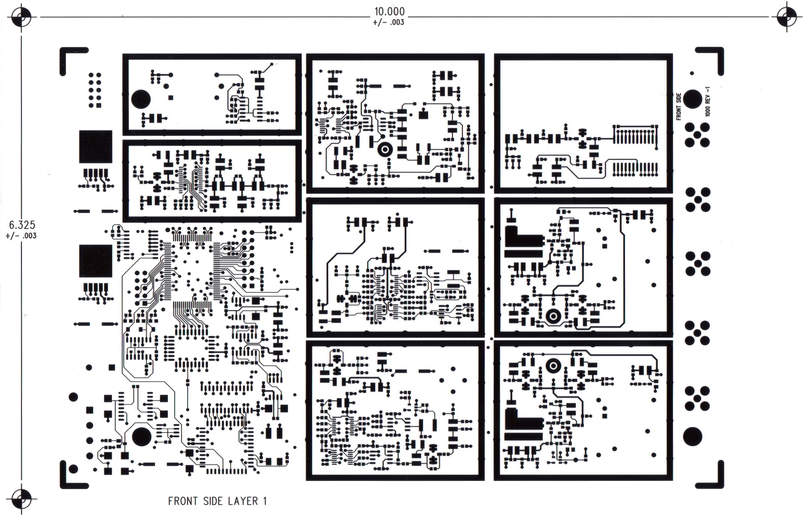
| Multilayer High Frequency / High Isolation Printed Circuit Card Design | |
Hover mouse over layer:Layer 3: StripLine / Box only routing Layer 4: Gnd Plane(negative) Layer 6: Gnd Plane(negative)
|
 |
| Multilayer High Frequency / High Isolation Printed Circuit Card Design | |
Hover mouse over layer:Layer 3: StripLine / Box only routing Layer 4: Gnd Plane(negative) Layer 6: Gnd Plane(negative)
|
|